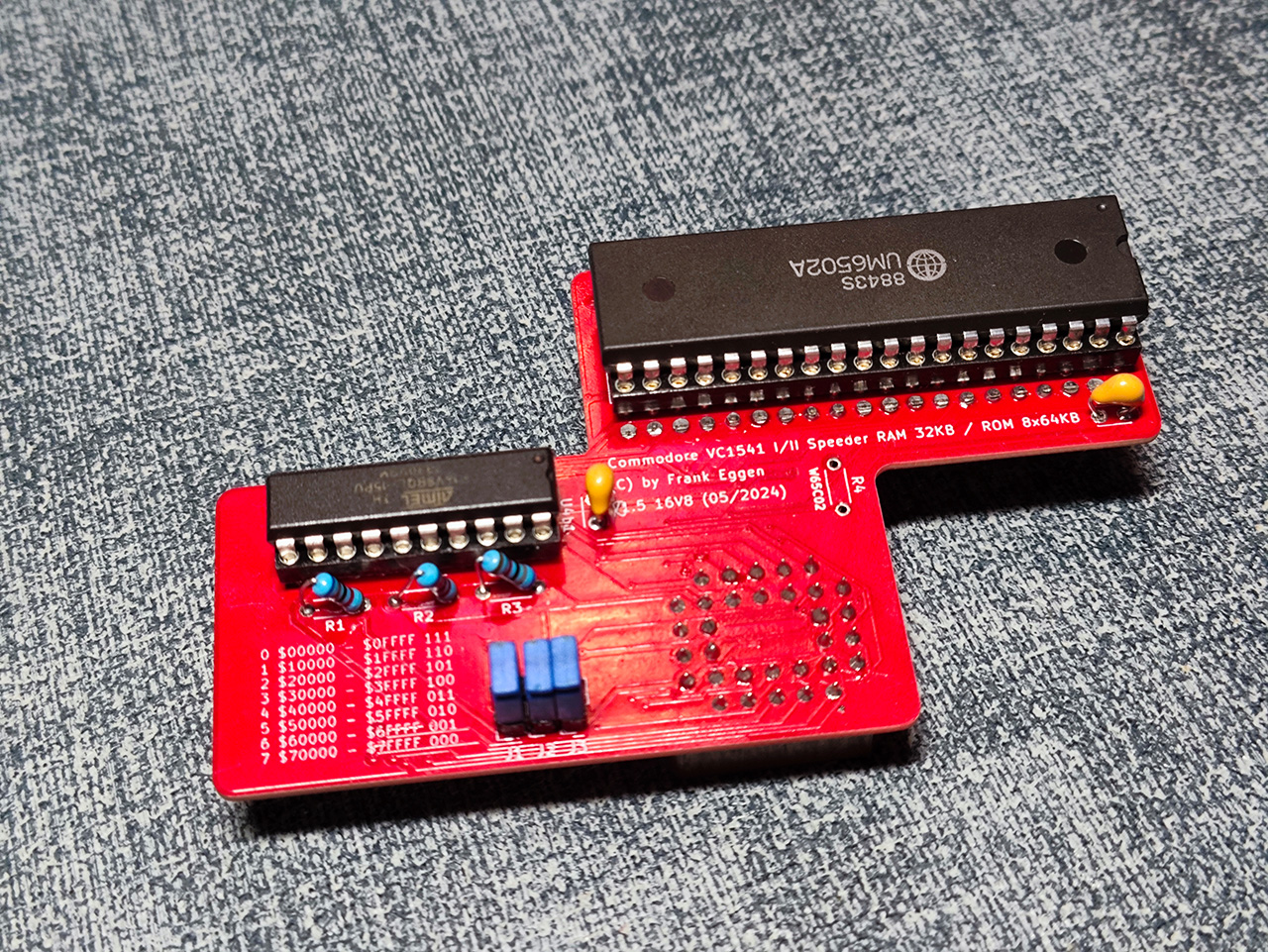
My Multi-Speeder project for the Commodore 1541 disk drive consists of an expansion board that is inserted between the 6502 CPU. The board expands the 1541's memory by 32 KB and provides 8x 64 KB banks for DOS operating systems on the 1541. The expansion board can be used with both the 1541-I and 1541-II versions. I have also designed a version for the Oceanic OC-168 clone (available on request).
With the Multi-Speeder expansion board, systems like the original CBM-DOS 2.6, DolphinDos 2.0, SpeedDos 2.7+, SpeedDos Expert, JiffyDOS, and S-JiffyDOS can be switched and used.
The addressing of the ROM and RAM areas varies, allowing the Multi-Speeder to be used with different floppy speeders.
A SpeedDos-compatible parallel cable for the C64’s user port and a ROM adapter socket for the C64 Kernals are not included in this project. These can be purchased from well-known retro shops, such as Faszination64 (see links below).
I have provided the schematic, the corresponding EPROMmer file for the ATF16V8 (GAL16V8 compatible) address decoder, and the Gerber files, e.g., for PCBWay. This allows you to produce the Multi-Speeder board yourself.
In addition to the board, the following components are required:
- 2x Precision Pin Header 20-pin, 2.54mm (Board to Mainboard)
- 1x IC Socket, 40-pin (for U1) (6502 CPU)
- 1x IC Socket, 20-pin (U4b1) (Atmel F16V8 BQL-15PV) (GAL16V8 compatible)
- 1x IC Socket PLCC 32, 32-pin (EEPROM/EPROM)
- 1x IC Atmel F16V8 BQL-15PV (U4b1) (Address decoder)
- 1x IC SRAM HM62256ALF-70G 28-PIN SOP or ISSI 62C256AL-45ULI 28-PIN SOP
- 1x EPROM-OTP AT27C040-70JU or AM27C040-120LC (PLCC32) or EEPROM 29F040 (PLCC32) (from version 1.6, set the appropriate solder bridge!).
- 2x Tantalum Capacitor, 100 nF radial (C1 and C2)
- 3x Resistors 4.7 kOhm / 1/4 Watt (R2, R3, R4)
- Optional 3.3 kOhm (R1 is only optional for a WDC65C02 CPU and is not required for an original MOS 6502!)
- 3x Jumpers (JP1, JP2, JP3)
- 2x 3x1 Header Pin-Pin
On the board from version v1.5 onwards, the resistor R4 does not need to be installed, and JP1 remains closed. These are only intended for test operation with a newer WDC W65C02 CPU.
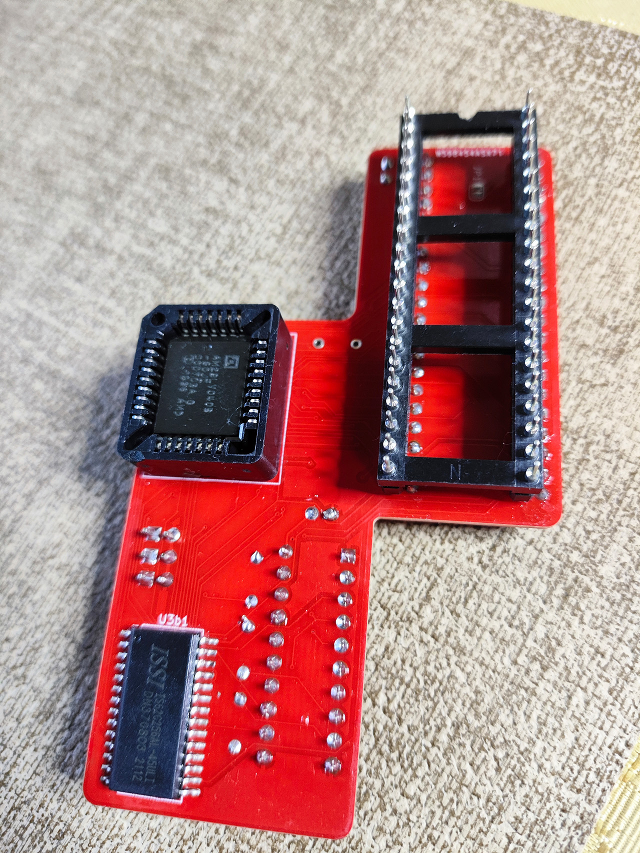
You can use an EPROM-OTP 27c040 or a Flash-EPROM 29F040. Please ensure that the respective jumper JP5 or JP6 is set! Otherwise, the bank switching will not work correctly, as the pin layout of these EPROM types slightly differs (PIN 1/PIN 32).
The DOS Kernals are stored in an EPROM. The EPROM, e.g., 27C040/29F040, is a 512 KB EPROM. It is divided into 8x 64 KB banks (Bank 0-7). Each bank $x0000 - $xFFFF mirrors the 64 KB memory area of the floppy drive 1:1. However, only a specific portion of the areas is mapped into the memory area of the 1541 (see the table below). This does not fully utilize the capacity of the EPROM but makes address decoding and configuration very simple and flexible. Furthermore, memory is no longer as expensive as it was in the 1980s :-). When using the Multi-Speeder board, all original ROM ICs of the 1541 must be removed or deactivated (CS/CE/OE permanently high) as they would otherwise conflict with the Multi-Speeder ROM in the address space. The result would be a crash of the floppy drive immediately upon startup.
BANK 0-7 $2000 - $FFFF
From Address Decoder 2.0, the ROM is generally mapped into the 1541 from address $2000 to $FFFF. Only the RAM area overlays the ROM. The advantage is that it allows additional Kernal routines to be placed in the 1541.
Just like the ROM, the 32K RAM is also mapped into various areas of the 1541. Where the RAM is mapped depends on the bank that is currently active.
| ROM Bank | ROM Area | CPU RAM Area(s) | Kernal |
|---|---|---|---|
| 0 | $00000-$0FFFF | $2000 - $9FFF 32 KB | CBMDOS 2.6 |
| 1 | $10000-$1FFFF | $2000 - $9FFF 32 KB | DolphinDos 2.0 |
| 2 | $20000-$2FFFF | $2000 - $9FFF 32 KB | SpeedDos+40T |
| 3 | $30000-$3FFFF | $2000 - $9FFF 32 KB | JiffyDos 5.0 |
| 4 | $40000-$4FFFF | $2000 - $7FFF 24 KB | S-JiffyDos 1 |
| 5 | $50000-$5FFFF | $2000 - $7FFF 24 KB | CBMDOS 2.6 (Placeholder) |
| 6 | $60000-$6FFFF | $A000 - $BFFF 08 KB | CBMDOS 2.6 (Placeholder) |
| 7 | $70000-$7FFFF | $A000 - $BFFF 08 KB | SpeedDos 2.7 Expert |
In the /software/ directory, there is a diagnostic tool for the C64 to test the 32K RAM of the Multi-Floppy Speeder. The memory locations from $6000 to $9FFF are first written with $00 bytes and then with $FF bytes. Any errors encountered are displayed. This test should always be performed with BANK0 and the original CBMDOS. The tool is available for . The tool is useful for testing whether the RAM chip is functioning correctly after soldering.
In the 1541, Commodore economized on the address decoder. The VIAs ICs at $1800 and $1C00 are mirrored across the address ranges up to $8000. This collides with the RAM expansion. I resolved this issue by adjusting the A15 address line on the board and connecting it to the motherboard. This stops the mirroring issue for the RAM, so nothing collides from address $2000 onwards in the 1541.
 Here is an example of operation in an older 1541-I. The 6502 CPU, address decoder, and EPROM are socketed. There is enough space here. This is an older version 1.1, and the EPROM is mounted on top of the board. From version 1.4 onwards, the EPROM is located on the underside of the board.
 In contrast to the older 1541-I
, the 1541-II is much more compactly built. The board is located under the drive mechanism. Therefore, there is little space for expansions. For this reason, I solder the CPU (U1) and the address decoder (U4b1) directly onto the board without using an IC socket. This way, the board can be plugged into an IC socket on the 1541-II’s mainboard without interfering with the drive mechanism.
The cables on the left (Yellow, Green, Blue) (DIP1) set the active bank. A DIP switch or binary switch can also be used here. However, it doesn’t make much sense for the 1541-II since you don’t have access during operation. In this example, I have placed a binary switch outside via a cable. This connects these contacts to ground GND (0). Without a switch, the address lines A16/A17/18 are at +5V (1), and Bank 7 is active. If the three contacts on DIP1 are connected to ground GND (0), then Bank 0 is active. Starting with version v1.6, I no longer use a DIP switch but three jumpers.
- My PCBWay.com Shared Project Page
- Board Gerber Files
- JED File for ATF16V8 (GAL16V8)
- Images
- Schematic
- Board
- Faszination64: Retro Parts like 1541 Userport-Parallel Cable and C64 ROM-Kernal Adapter
From board version v1.5 onwards, a new WDC W65C02 CPU can also be used. However, the optional resistor R1 (3.3K) must be installed, and JP4 must be opened! However, this reduces the 1541’s compatibility. The original CBM-DOS runs, but most floppy speeders also use illegal opcodes of the original old MOS 6502A CPU, which the newer WDC W65C02 CPU does not recognize. As a result, much software that uses fast loaders with illegal opcodes will not work. That’s why I am still looking for an FPGA emulation that can be used for my Multi-Speeder instead of an original MOS 6502A CPU. Rockwell 6502 CPUs and those from UMC and SY6502A also work without issues.
If you would like to support my work, I would appreciate a donation via PayPal. > Donate <
I take great care and pride in my work. However, I cannot rule out errors. This is a hobby project, and I do not take any responsibility for the functionality or for any consequences that may arise from modifying/installing my projects in your devices. I also accept no liability for possible consequential damages resulting from the described correct use of my board.
I still hope you enjoy it, and I am always open to suggestions or improvements. As mentioned earlier, if anyone has built a compatible FPGA MOS 6502 CPU, please get in touch :-)))
V1.7 from 20.06.2024
- BOM updated.
- Address decoder V1.7 optimized. ROM mapping for BANK 6-7 extended from $8000 - $8FFF to $8000 - $9FFF.
- RAM footprint optimized.
- Labels for JP1-JP3 corrected (inverted).
- PCB labeling optimized. (TOP/BACK) PIN-Header framed on the back.
V1.7 from 26.07.2024
- Change from 29LV040 to 29F040 EPROM
V1.7a from 09.08.2024
- A new, better footprint for the SRAM to make it easier to solder and the EPROM in a PLCC socket on top of the PCB.
V1.7a
- Update ATF16V8 Address Decoder to Version 2.2b.
- Update Readme
Best regards,
Frank